
Oximem - RAEng Chair in Emerging Technologies
Scaleable Ultralow Power Memory through Materials Innovation
Together with the ERC Advanced Grant, Prof. Driscoll's RAEng Research Chair in Emerging Technologies provides the largest amount funding for our current research. In this project 'Oximem', we investigate oxide thin films for resistive switching with applications in a wide range of data centric technologies spanning IoT, transport, medicine, security, entertainment, neuromorphic computing, and AI, all of which will evolve significantly over the next decade, and in time will radically change the way we live. A broader overview over the field of research is provided here, and on this page, we provide more information about the project-specific approach.
Project Details
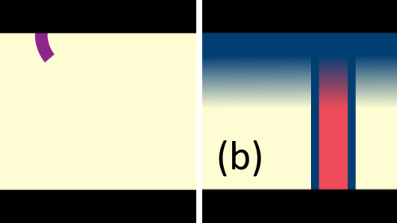
One of the most widely researched approaches to resistive switching relies on amorphous oxide materials, where different resistive states are realised by the state of a filament, which is formed by oxygen vacancies or metal ions. The formation of such a filament between two electrodes results in the 'low resistive state' (LRS), whereas the rupture of the filament results in the 'high resistive state' (HRS). This is illustrated in Fig. 1 (a). Since the migration of ions in an amorpous material is intrinsically random, filamentary memory cells exhibit large degrees of variability, which is detrimental to reliable memory operation. In this paper, in a model materials system, we demonstrated that the migration of ions in oxide thin films can be directed in a way that eliminates the intrinsic randomness and leads to stable an reproducible resistance states (LRS and HRS). This approach relies on the precision engineering of self-assembled oxide films to create controlled and separate channels for ionic and electronic conduction. In such films, the resistance will be controlled by an energy barrier at the interface of the oxide film via the accumulation or depletion of oxygen vacancies. This is illustrated in Fig. 1(b).
In this project, we pursue two main goals:
(1) Engineer well-controlled electronic and ionic channels in industrially compatible oxide films, such as HfO2.
(2) Control the concentration of oxygen vacancies in the films to tune their conductivity and thus resistance levels.
Stable resistive switching in oxide films fulfilling these goals will enable swift commercialisation of our technique to pave the way for energy-efficient non-volatile memory in consumer applications. This will benefit the environment and end users alike, since it will lead to longer battery life times and consequently less greenhouse gas production.
The required precision engineering is achieved in the fabrication step of our oxide thin films. Our group has many years of experience in thin film fabrication by pulsed laser deposition, sputtering, and spatial atomic layer deposition and we have demonstrated the feasibility of defining controlled conduction paths.
The Team
The core team for this project consists of Prof. Driscoll, Dr. Ming Xiao, and PhD student Thomas Sun. Thomas focuses spatial atomic layer deposition and structural characterisation, while Ming fabricates thin films by sputtering, leads the electrical characterisation efforts, and supports Prof. Driscoll with the organisation and supervision of the project.
Besides this core team, many other group members, funded by other sources, interact with the project to maximise the shared competence. They are Dr. Markus Hellenbrand (ECCS-EPSRC), Dr. Nives Strkalj (SNF fellow), Dr. Megan Hill (Herchel Smith fellow), Dr. Max Becker, and PhD students Moritz Müller (EPSRC nanoDTC) and Mahmoud Elshenawy (funded by the Winton Programme).
Team Capabilities
With the comprehensive interaction of many group members, our team covers a wide range of expertise in thin film growth, materials characterisation, and devices fabrication and testing.
| Growth Capabilities | Device Fabrication | Electrical characterization | Spectroscopy | Surface imaging | Microscopy |
| PLD, Sputtering, ALD | Sputtering, evaporation, lithography | DC, RF, ferroelectric testing, impedance measurements | Nanoplasmonic optical spectroscopy, environemntal XPS, in-situ XPS, synchrotron based XAFS | AFM, CAFM, PFM | STEM, nano-focused X-ray imaging (diffraction, XAFS) |
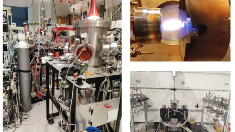
The photographs to the right present some of our thin film deposition facilities. The large picture is a view into our laser lab with several chambers for pulsed laser deposition. A view into the vacuum chamber in the foreground during deposition provides a stunning view of the plasma plume generated by the pulsed laser beams, top right image. The bottom right image shows one of our custom-build spatial atomic laser deposition setups.
We have access to a large X-ray diffraction lab with several different diffractometers to match the characterisation requirements of different films and materials. For surface characterisation, we can employ atomic force microscopy and piezoresponse force microscopy. Our electrical characterisation suite es equipped with custom-programmed source measure units, impedance analysers, and a dedicated ferroelectric tester. In collaboration with the Division of Electrical Engineering and the Henry Royce Institute, we also have access to high speed electrical characterisation equipment, and in collaboration with Dr. Di Martino's lab, we can characterise resistive switching by in situ nanoplasmonic spectroscopy.